Atomic force microscopy (AFM)/Raman is the latest trend in hybrid imaging/chemical analysis instrumentation. 1–4 Enjoying a rapid rise to prominence over the past two years, manufacturers now offer fully integrated systems as well as interfaced systems, marrying independent AFMs and Raman spectrometers, making this technique available to the routine laboratory either as a full system or as an add-on.
Initially the purview of physicists, AFM/Raman is now seen as a valuable tool for pharmaceutical companies; cell and molecular biologists seeking to link structure with drug or metabolic interactions; chemists working with films, monolayers, and multiphase systems; and designers of new materials, especially in nanotechnology, all of whom need to coordinate chemical information with phase distribution, electrical, mechanical, or magnetic information.
Principles
Atomic force microscopy is a member of the larger class called scanning probe microscopy (SPM). In the simplest sense, an SPM operates very much like a phonograph, scanning an atomically sharp tip over the surface of interest in a variety of motions ranging from contact to semicontact and noncontact. Depending on configuration, the tip:surface interaction can sense, and therefore image, diverse information, including topography; location of phases; differences in local elasticity and work function; magnetic fields; and electrical fields dependent on voltage, current, or resistance.5 Magnification can be changed by varying the size of the field scanned.
Raman spectroscopy detects changes in the vibrational state of the atoms within a susceptible molecule. A photon, typically generated by a laser, excites an electron, causing a change in vibrational state. Upon relaxation, part of the excitation energy is released in the form of a signature spectrum in the 0–4000 cm–1 range (approximately 2–10,000 μm). When used in connection with either optical or atomic force microscopy, the Raman spectrometer is fitted with a confocal slit or pinhole, to define the exact plane from which the spectrum is collected. Combining AFM with Raman opens new opportunities for correlating chemical information with other physical, electrical, and magnetic properties.
Interface or integrate?
The NTegra Spectra (NT-MDT, Zelenograd, Russia) leads the field for fully integrated AFM/Raman systems. Built around a high-resolution Solare spectrometer and the highly modular NTegra AFM, it offers motorized controls for the confocal apertures; choices between as many as three different lasers; and multiple dichroics, all easily managed through the same Nova software that runs the AFM. For transmitted light applications, it fits neatly on an Olympus IX-71 microscope (Melville, NY), also providing convenient expansion to nearfield scanning optical microscopy (NSOM). In total, the system offers light and confocal microscopy; more than 40 different AFM/SPM modes; NSOM; and both confocal Raman and fluorescence spectroscopy, all controlled through one piece of software—Nova.
For facilities that already own a Raman spectrometer or practitioners who prefer a specific brand, many of the AFM companies now offer interface options. NTegra has already been mated with both the Renishaw InVia (Wotton-under-Edge, U.K.) and with the Horiba-JY LabRam (Edison, NJ). However, in most instances, the interface is primarily physical. The spectrometer is still run on its own software and the AFM run on its software, with the ability to import spectra.
“Seeing around corners”—the Holy Grail for reflected light samples
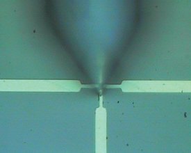
Figure 1 - The high aperture head “sees around corners,” ensuring that the Raman and AFM information come from exactly the same location. It also provides simple interfacing to other spectrometers.
Reflected samples have been more of a challenge for AFM/Raman systems. To answer that challenge, NT-MDT designed the high aperture (HA) head. As shown in Figure 1, the optics essentially render the normally opaque tip transparent and ensure that the Raman signal comes from exactly the same location as the AFM image. In addition to extending AFM/Raman to opaque samples, HA also provides a facile link for interfacing.
Experimental expectations
All Raman experiments face several key challenges, notably, Raman signal strength and locating Raman peaks that are not masked by often-present fluorescence. Today’s spectrometers optimize signal collection through thoughtful use of adjustable entrance slits, holographic gratings, and notch filters.
Combining AFM with Raman presents a different set of challenges. While not significant, they are best met with realistic expectations. The first of these is the difference in acquisition time: AFM images typically take tens of seconds, while the Raman spectra can require hours. To conduct combined AFM/Raman experiments, the systems must be extremely stable, with feedback electronics and devices such as the HA to ensure that the Raman information is, indeed, collected from exactly the same AFM location.
A second issue is spatial resolution. AFM images structures ranging from approximately 100 μm (XY) down to the atomic level, while Raman is diffraction limited and, in conventional mode, is limited to structures approximately 250–300 μm in size. Pioneering efforts are now under way using tip enhanced Raman spectroscopy (TERS), improving the spatial resolution to approximately 50 μm. While the NTegra Spectra is TERS-ready, the experiments are not trivial.
Finally, because AFM is a scanning technique, it is extremely sensitive to vibration. Two critical sources of vibration in an AFM/Raman setup are the multiple lasers and, ironically, compressors for the antivibration table. The simple solution is to relocate these sources of tremor and, for lasers, to use solid-state lasers instead of gas-cooled varieties.
Applications
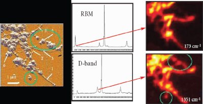
Figure 2 - AFM image, Raman spectra, and Raman images of single-walled carbon nanotubes. Amorphous carbon is visualized in the D-band (1351 cm–1), while well-structured nanotubes are present in the RBM-band (173 cm–1). Raman images size 5 × 5 μm. (Images courtesy of Dr. Igor Kudryashov, TII, Tokyo, Japan.)
As the tools for AFM/Raman have become more readily available and easier to use, the diversity of AFM/Raman applications has begun to expand. Carbon nanotubes are a favorite target. Figure 2 shows the AFM image accompanied by the Raman images and corresponding spectra, taken at two different wavelengths.
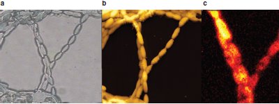
Figure 3 - Algal cells. a) Light microscopy/phase image; b) AFM image; and c) Raman image, showing location of β-carotene just on the surface. (Sample courtesy of Dr. D. McNaughton, Monash University, Victoria, Australia. Images courtesy of Dr. Paved Dorozhkin, NT-MDT.)
Figure 3a and b compare the information from conventional light microscopy (phase contrast) to AFM imaging of an algal cell. The accompanying Raman image (Figure 3c) shows that the protein, β-carotene, is localized primarily on the surface of these cells.
Summary
AFM/Raman is opening exciting new avenues in research as well as industrial characterization across a wide array of fields. In biology, this combination has imaged and collected spectra from single molecules. In semiconductors, it has been used to map the location of germanium in doped silicon and, using the high resolution of today’s spectrometers, to detect delicate strain in silicon crystals. In nanotechnology, it has easily characterized and imaged carbon nanotubes, as well as activated and mapped the light transport in nanowires. It is the next logical step in the powerful convergence of imaging and spectroscopy, dramatically expanding the analyst’s toolbox.
References
- Foster, B. Focus on microscopy: convergence of technologies and companies drive new directions in microscopy. Am. Lab.1999, 31(14), 48–53.
- Foster, B. Focus on microscopy: from light microscopy to molecular analysis at the touch of a button. Am. Lab.2001, 33(22), 42–9.
- Foster, B. Raman microscopy: taking chemical microscopy to the next level. Am. Lab.2003, 35(8), 18–23.
- Foster, B. Focus on microscopy: AFM’s new nanotomography expands 3-D imaging. Am. Lab.2005, 37(10), 42–4.
- Animations of these techniques are available at www.nanotech-america.com.
Ms. Foster is President of Microscopy/Marketing & Education, 313 S. Jupiter Rd., Ste. 100, Allen, TX 75002, U.S.A.; tel.: 972-954-8011; fax: 972-954-8018; e-mail: [email protected].