Engineered materials abound in products that we use every day. They can range from a bulk material like the glass in a window to a dispersion of titanium dioxide nanoparticles in a sunscreen formulation. Every material, from the plastic in the sole of a running shoe to the semiconductor chip in a laptop, has undergone a development process that includes an iterative cycle of characterization and performance testing. By gaining insight into the structure and composition of a material and linking that knowledge to properties that govern performance, designers can build better products while shortening development time.
Demands for improved product performance continually evolve. We want things that are smaller, lighter, faster, stronger, and greener. As performance specifications tighten, the need to understand and design materials moves from the bulk to the atomic level. Microscopy in all of its forms can provide insights into key material characteristics, elucidating size, texture, morphology, crystallinity (or lack thereof), elemental composition, and electronic state, at scales ranging from several micrometers to single atoms. Perhaps surprisingly, microscopes at two ends of the resolution scale, the light microscope and the transmission electron microscope, are very similar in function and in the types of information provided. A comparison of some key features will illustrate this similarity, and will also demonstrate why microscopy tools and techniques are central to materials characterization.
Figure 1 shows schematic cross-sections of imaging modes for three types of microscopes regularly used for materials characterization: the light microscope (left), the transmission electron microscope (TEM, center), and the scanning electron microscope (SEM, right). Common elements include an illumination source (a source of visible light or an electron gun) and a condenser lens above the specimen to focus the light or electron beam. After the condenser lens, the configuration of the SEM diverges from that of the light microscope and the TEM. In the latter two, the objective lens that forms the image is positioned below the specimen, and a static, near-parallel beam of illumination is projected onto a viewing point or onto a camera for recording. Though the TEM incorporates some additional lenses, the overall process by which the image is created and projected for viewing and recording is identical to that of the light microscope.
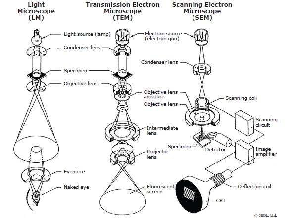 Figure 1 – Schematic cross-sections of imaging modes in the light microscope, the TEM, and the SEM (JEOL).
The SEM differs significantly in that the objective lens sits above the specimen, and the beam is formed into a fine, focused probe that is rastered across the specimen using scanning coils, building up an image point by point. The image can be recorded on various detectors positioned above the specimen.
These three types of microscopes provide complementary information over different size ranges. The unaided human eye can resolve features down to about 100 μm in size, and the best light microscopes allow us to see features as small as 1 μm. Because SEMs and TEMs utilize electrons, which have higher energies and shorter wavelengths than visible light, much smaller objects can be resolved. The highest-resolution SEMs can now distinguish features a few nanometers in size, while aberration-corrected TEMs allow for imaging and analysis at the atomic level. All three types of microscope can be used to provide fundamental information about size, morphology, and texture of materials, as shown in Figure 2. Though the SEM and TEM are typically grouped together as electron optical instruments, the TEM and the light microscope share a common mechanism for image formation.
 Figure 2 – Images of metal particles on a fiber support. Light microscope (top left), SEM (top right), TEM (bottom left, McCrone Associates). High-angle annular dark-field image of metal particle acquired on the TEM operated in scanning transmission mode. Arrow indicates single atoms of metal (bottom right, University of Illinois at Chicago).
Crystallographic analysis
Interaction of energetic wave sources such as light, X-rays, or electrons with the regularly spaced planes of atoms in a crystalline specimen generate patterns containing useful structural information. The type of pattern and the amount of detail provided about the crystal structure will vary with the technique used; some examples are shown in Figure 3. In an SEM equipped with a detector for electron backscatter diffraction (EBSD), a Kikuchi pattern that shows crystallographic orientation can be obtained; one common application is mapping of different orientations in a polycrystalline material. When coupled with elemental analysis by energy dispersive X-ray spectrometry (EDS) in the SEM, a Kikuchi pattern can be indexed to identify the crystal system of a material. The diffraction mechanism, Bragg scattering, is the same as in the TEM, but the pattern is formed by electrons backscattered from near the surface of the sample. The pattern is captured on the fluorescent screen of the EBSD detector.
 Figure 3 – Examples of crystallographic data. Light microscope interference figure from calcite (top left, McCrone Atlas of Microscopic Particles, www.mccroneatlas.com). SEM EBSD pattern from nickel (top right, Oxford Instruments). TEM SAED and CBED patterns from silicon (bottom left and right, University of Illinois at Chicago).
The TEM and the polarized light microscope again are more similar because both take advantage of the fact that crystallographic information is present in the back focal plane of the objective lens. In the polarized light microscope, light propagated in different directions through an anisotropic crystal structure forms an interference figure when the crystal is viewed through crossed polarizers. A Bertrand lens inserted into the light path is used to bring the image of the interference figure into focus in the focal plane of the eyepiece lens. The symmetry of the interference figure identifies the crystal system and the orientation of the crystal.
In the TEM, no additional detector is required to view diffraction information. The push of a button changes the configuration of the microscope lenses to project the diffraction pattern present in the back focal plane of the objective lens onto the viewing screen or camera where the image would be focused in imaging mode. This parallels use of the Bertrand lens in the polarized light microscope to move the interference figure from the back focal plane to a point where it can be observed.
The TEM pattern results from transmission of diffracted electrons through a thin specimen. In the TEM, Kikuchi patterns analogous to SEM EBSD patterns are used primarily for tilting the sample to the proper orientation to acquire high-resolution lattice images and other types of diffraction patterns that provide more detailed information. These include selected area electron diffraction (SAED) patterns, from which atomic plane spacings (d-spacings) and angles can be measured for matching to those of known materials. When combined with EDS analysis in the TEM, SAED patterns can be used for crystalline phase identification. The highest spatial resolution diffraction technique in the TEM is convergent beam electron diffraction (CBED), which yields much more detailed information: the unit cell and associated lattice parameters, crystal system identification, and three-dimensional crystal symmetry, including the point group and space group. CBED and observation of interference figures in the light microscope are both conoscopic techniques, utilizing converging beams (cones) of illumination.
Elemental and chemical identification and response to conditions
As noted above, elemental analysis is possible in electron optical instruments equipped with detectors for EDS. Interaction of primary beam electrons with core shell electrons in the atoms of the sample leads to emission of X-rays with energies characteristic of the elements present. A spectrum of peaks corresponding to specific X-ray energies is generated, and the peak intensities reflect relative elemental concentrations. In the SEM and TEM, EDS data can be gathered from selected areas or features to determine composition associated with different textures, morphologies, or crystalline phases. Areas analyzed may range from several micrometers to sub-nanometer in size.
In the light microscope, a variety of microchemical tests and reactions to various conditions can assist in the identification of materials. Techniques include solubility tests, replacement reactions, spot tests, and recrystallizations. Observation of reactions to heat and flame can include burning, melting, sublimation, explosion, decomposition, loss of hydration, or no reaction. These and other techniques done on a micro-scale using the light microscope foreshadowed the development of in situ techniques in electron optical instruments such as the environmental SEM, or the TEM equipped with environmental holders or with modifications to the microscope that allow for viewing of samples in reactive environments.
Inclusion of techniques for compositional analysis strengthens the power of any microscopy technique, confirming preliminary identifications based on imaging and crystallographic results. When observations are taken to the next level and carried out in controlled environments that reflect conditions of use in the real world, an even better understanding is gained between a material’s structure and properties, with an improved ability to predict and control performance.
Quality of results and an integrated approach
Regardless of the type of microscope used, calibration, performance verification, and good maintenance practices are vital for ensuring quality of results. However, no matter how good the instrument or the analyst, the nature of the specimen will drive the characterization process and ultimately determine the quality of the results obtained. Sample preparation techniques will be more or less rigorous depending on the type of microscopy used, but representative sampling and minimization of artifacts introduced by preparation must be considered, regardless of the scale at which one is working. Also, the higher the magnification, the smaller the field of view, necessitating more time to examine enough areas to ensure that results are representative. While 15 minutes may be sufficient for identification of a material using light microscopy, analysis times of at least an hour per sample, and often much longer, are common for TEM analysis. Because small volumes of material are examined by any microscopic technique, using microscopy at different scales and comparing results with those obtained from bulk analyses should always be considered. This integrated approach will provide the most accurate and comprehensive insights into the nature of a material.
Summary
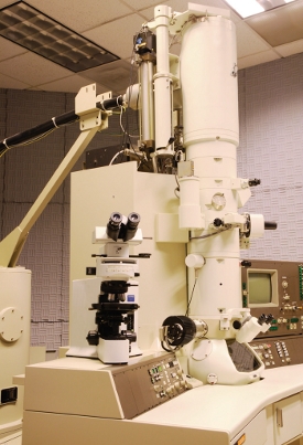 Figure 4 – Polarized light microscope (Olympus BX51) and TEM (JEOL JEM-3010): more similar than they appear.
Two of the most enjoyable aspects of any form of microscopy are the interactive nature of the analysis and the fact that multiple techniques can be employed in a single instrument. Analysis in the microscope is a decision-making process that begins with some amount of knowledge about the material, and usually with some specific questions to be answered using microscopy. As the nature of the sample is revealed by examination of a succession of areas and features, the preliminary analysis plan may change, and the analyst may select from among the multitude of imaging, crystallographic, and compositional techniques that microscopy provides, to gather the most relevant and representative data.
This brief discussion of microscopes at two ends of the resolution scale does not even begin to touch on the vast array of specialized microscopes and associated techniques available today for materials characterization. However, even this simple overview of similarities between the light microscope and the TEM, shown together in Figure 4, illustrates the wealth of information that can be gathered using microscopy, and the vital role it plays in characterization and development of today’s high-performance materials.
Elaine F. Schumacher is a Senior Research Scientist at McCrone Associates, Inc., and co-teaches a TEM course at Hooke College of Applied Sciences, LLC, 850 Pasquinelli Dr., Westmont, IL 60559, U.S.A.; tel.: 630-887-7100; e-mail: [email protected]; www.mccrone.com